®
Virtual
Great • Alfred • Nobel • Gives • Aspiration!
Nobel & Laureates' Ideas & Thought Processes!
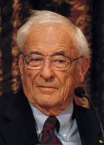
Willard Boyle Ph.D.
Willard Boyle Ph.D.
The Nobel Prize in Physics 2009
Co-nobelists: Charles K. Kao, George E. Smith
Prize motivation: "for the invention of an imaging semiconductor circuit - the CCD sensor."
Patents
| Publication: | 1/16 |
| Publication No: | US 3858232 A |
| Title: | Information storage devices |
| Publication Type: | Grant |
| Publication Date: | December 31, 1974 |
| Filing Date: | November 9, 1971 |
| Inventors: | Willard Boyle, George Smith |
| Original Assignee: | Bell Telephone Labor Inc |
| Abstract: | The specification describes devices based on the recognition that minority charge carriers within a semiconductor can be used to represent information. Storage sites are provided by potential wells formed along the semiconductor surface. The preferred structure is an array of metal electrodes on an insulating layer, each electrode comprising an MIS device. A quantum of charge carriers, representing an information bit, is generated within the semiconductor. This quantum can be translated along the semiconductor by successively biasing a row of electrodes. The potential well effectively "moves" through the semiconductor sweeping the minority carriers with it. The quantum can be detected by a simple capacitive couple, e.g., a floating gate FET. |
Representative Figure: | |
| Family | |
| Details | Google Patents USPTO Patent Database |
| Publication: | 2/16 |
| Publication No: | US 3796927 A |
| Title: | Three dimensional charge coupled devices |
| Publication Type: | Grant |
| Publication Date: | March 12, 1974 |
| Filing Date: | December 16, 1970 |
| Inventors: | Willard Boyle, George Smith |
| Original Assignee: | Bell Telephone Labor Inc. |
| Abstract: | The specification describes a new class of semiconductor devices in which the charge is controllably translated in three dimensions. Translation control circuits can be disposed on both sides of the usual semiconductor wafer giving a new dimension in the design of logic and memory devices. In the exemplary specific embodiment the concept is described in connection with a shift register. Extension to logic circuits, e.g., to perform crossover and fan-in functions, is straightforward. |
Representative Figure: | |
| Family Members | CA946076A1, DE2162140A1 |
| Details | Google Patents USPTO Patent Database |
| Publication: | 3/16 |
| Publication No: | US 3792322 A |
| Title: | Buried channel charge coupled devices |
| Publication Type: | Grant |
| Publication Date: | February 12, 1974 |
| Filing Date: | April 19, 1973 |
| Inventors: | Willard Boyle, George Smith |
| Original Assignee: | Willard Boyle, George Smith |
| Abstract: | The specification describes charge coupled devices in which the storage layer is internally charged so that the energy level profile across the thickness of the layer has a maxima in the middle of the layer. Injected carriers can then be stored and transferred in the bulk region of the semiconductor. If the energy level of the maxima exceeds the surface energy of the valence band by an amount exceeding the Boltzmann expression for thermal excitation, then the stored carriers remain isolated (statistically) from the surface states. The storage layer can be appropriately charged by biasing the layer to remove the mobile carriers. Residual fixed charge bends the energy band if the boundaries are fixed to appropriate barriers. The most convenient structure appears to be a large area p-n junction for the lower (buried) barrier with the usual MIS surface barrier. An MISIM structure is predictably similar. Multichannel structures are proposed such as N-P-N-P-N in which the isolated P-channels serve simultaneously as storage layers. Simultaneous use of both channels with controlled interconnection suggests many potential applications for logic circuits and the availability of convenient crossovers. |
Representative Figure: | |
| Family | |
| Details | Google Patents USPTO Patent Database |
| Publication: | 4/16 |
| Publication No: | US 3581151 A |
| Title: | Cold cathode structure comprising semiconductor whisker elements |
| Publication Type: | Grant |
| Publication Date: | May 25, 1971 |
| Filing Date: | September 16, 1968 |
| Inventors: | Willard Boyle, Jack Morton> |
| Original Assignee: | Bell Telephone Labor Inc |
| Abstract: | Cold cathode structures comprise a plurality of semiconductor whisker elements each including an electronic barrier near the free end. Electron emission is enhanced by a high external field that is concentrated at the tip of each whisker element. |
Representative Figure: | |
| Family | |
| Details | Google Patents USPTO Patent Database |
| Publication: | 5/16 |
| Publication No: | US 3551213 A |
| Title: | Geometrically selective ion bombardment by means of the photoelectric effect |
| Publication Type: | Grant |
| Publication Date: | December 29, 1970 |
| Filing Date: | September 4, 1968 |
| Inventors: | Willard Boyle |
| Original Assignee: | Bell Telephone Labor Inc |
| Abstract: | Geometrically selective ion bombardment of the surface of a target body, such as a semiconductor, is accomplished by means of the photoelectric effect. The body is placed in a gas containing the desired atomic species, while ultraviolet radiation is focused upon the surface of the target body in accordance with a desired pattern of bombardment. Photoelectrons are emitted from the surface and are accelerated away from the surface by an applied electric field. Finally, the photoelectrons ionize the gas, and the ions created thereby are accelerated back towards the surface of the target body. |
Representative Figure: | |
| Family | |
| Details | Google Patents USPTO Patent Database |
| Publication: | 6/16 |
| Publication No: | US 3502891 A |
| Title: | Variable reflectance memory device |
| Publication Type: | Grant |
| Publication Date: | March 24, 1970 |
| Filing Date: | March 22, 1967 |
| Inventors: | Willard Boyle, Jack Morton |
| Original Assignee: | Nasa, Smoot George F, Pope William L, Lawrence Smith |
| Abstract: | A memory module for use in logic or memory systems includes a variable reflectance device and a photosensitive member connected in a circuit, with the photosensitive member disposed to intercept light reflected from the reflectance device. The photosensitive member controls the reflective state of the reflectance device in response to ambient light and a scanning beam of energy. |
Representative Figure: | |
| Family | |
| Details | Google Patents USPTO Patent Database |
| Publication: | 7/16 |
| Publication No: | US 3473602 A |
| Title: | Apparatus and method for achieving temperature stabilization of a radiator using thermoreflectance materials |
| Publication Type: | Grant |
| Publication Date: | October 21, 1969 |
| Filing Date: | September 18, 1967 |
| Inventors: | Willard Boyle, Hans Verleur |
| Original Assignee: | Bell Telephone Labor Inc |
| Abstract: | When a radiating body (e.g. a satellite) is coated with a layer of a metallic reflector, a dielectric and a thermoreflectance material in the order recited, the temperature of the body is stabilized at the transition temperature of the thermoreflectance material. |
Representative Figure: | |
| Family | |
| Details | Google Patents USPTO Patent Database |
| Publication: | 8/16 |
| Publication No: | US 3434661 A |
| Title: | Snow making |
| Publication Type: | Grant |
| Publication Date: | March 25, 1969 |
| Filing Date: | February 1, 1966 |
| Inventors: | Willard Boyle, David Creaghan |
| Original Assignee: | David Creaghan, Willard Boyle |
| Abstract: | A method for making snow which comprises dispersing solid seeding particles in water and then spraying the water into the atmosphere at temperatures below freezing. |
Representative Figure: | |
| Family | |
| Details | Google Patents USPTO Patent Database |
| Publication: | 9/16 |
| Publication No: | US 3384794 A |
| Title: | Superconductive logic device |
| Publication Type: | Grant |
| Publication Date: | May 21, 1968 |
| Filing Date: | March 8, 1966 |
| Inventors: | Willard Boyle, George Smith |
| Original Assignee: | Bell Telephone Laboratories Inc |
| Abstract: | A superconductive logic device includes a superconductive layer in a portion of which superconductivity is induced by establishing a majority carrier density gradient in the layer while simultaneously maintaining constant therein the total carrier concentration. The transition temperature increases above the ambient temperature of the layer in the portion of the layer in which the majority carrier concentration is increased. Consequently that portion, which was initially in a normal resistive state, switches to a superconducting state. The logic device has application as a switch, a memory element and a level detector.. |
Representative Figure: | |
| Family | |
| Details | Google Patents USPTO Patent Database |
| Publication: | 10/16 |
| Publication No: | US 3354404 A |
| Title: | End pumped optical maser |
| Publication Type: | Grant |
| Publication Date: | November 21, 1967 |
| Filing Date: | August 29, 1961 |
| Inventors: | Willard Boyle, Donald Nelson |
| Original Assignee: | Bell Telephone Labor Inc |
| Abstract: | No Abstract |
Representative Figure: | |
| Family Members | DE1194978B|
| Details | Google Patents USPTO Patent Database |
| Publication: | 11/16 |
| Publication No: | US 3059117 A |
| Title: | Optical maser |
| Publication Type: | Grant |
| Publication Date: | October 16, 1962 |
| Filing Date: | January 11, 1960 |
| Inventors: | Willard Boyle, David Thomas |
| Original Assignee: | Bell Telephone Labor Inc |
| Abstract: | No Abstract |
Representative Figure: | |
| Family Members | USRE25632 |
| Details | Google Patents USPTO Patent Database |
| Publication: | 12/16 |
| Publication No: | US 2905820 A |
| Title: | Intermittent discharge pulse generators |
| Publication Type: | Grant |
| Publication Date: | September 22, 1959 |
| Filing Date: | July 20, 1954 |
| Inventors: | Willard Boyle |
| Original Assignee: | Bell Telephone Labor Inc |
| Abstract: | No Abstract |
Representative Figure: | |
| Family | |
| Details | Google Patents USPTO Patent Database |
| Publication: | 13/16 |
| Publication No: | US 2884565 A |
| Title: | Self-propagating intermittent discharge delay lines |
| Publication Type: | Grant |
| Publication Date: | April 28, 1959 |
| Filing Date: | September 16, 1954 |
| Inventors: | Willard Boyle, Raymond Ketchledge |
| Original Assignee: | Bell Telephone Labor Inc |
| Abstract: | No Abstract |
Representative Figure: | |
| Family | |
| Details | Google Patents USPTO Patent Database |
| Publication: | 14/16 |
| Publication No: | US 2864054 |
| Title: | Velocity measurement of relay contacts |
| Publication Type: | Grant |
| Publication Date: | December 9, 1958 |
| Filing Date: | March 19, 1957 |
| Inventors: | Willard Boyle, James Smith |
| Original Assignee: | Bell Telephone Labor Inc |
| Abstract: | No Abstract |
Representative Figure: | |
| Family | |
| Details | Google Patents USPTO Patent Database |
| Publication: | 15/16 |
| Publication No: | US 2836703 A |
| Title: | Low voltage arc welding circuit for use with percussion hand welder |
| Publication Type: | Grant |
| Publication Date: | May 27, 1958 |
| Filing Date: | June 19, 1956 |
| Inventors: | Willard Boyle, James Smith |
| Original Assignee: | Bell Telephone Labor Inc |
| Abstract: | No Abstract |
Representative Figure: | |
| Family | |
| Details | Google Patents USPTO Patent Database |
| Publication: | 16/16 |
| Publication No: | US 2802918 A |
| Title: | Electrostatic relay |
| Publication Type: | Grant |
| Publication Date: | August 13, 1957 |
| Filing Date: | April 29, 1955 |
| Inventors: | Willard Boyle |
| Original Assignee: | Bell Telephone Labor Inc |
| Abstract: | No Abstract |
Representative Figure: | |
| Family | |
| Details | Google Patents USPTO Patent Database |
Discover Your Abilities and Aspirations!
 $10 $25 $50 $100 Other
Tax Exempt 501(c)3 Non-Profit Organization
Any Currency
“One comes to be of just such stuff as that on which the mind is set” - Maithri Upanishath, VI.34:3
“…the peace that is found in libraries and laboratories…” - Louis Pasteur
“…the peace that is found in libraries and laboratories…” - Louis Pasteur
Contact Us E-Mail: info@GangaLib.org
Ganga library non-profit 501(c)(3) org. Contributions tax deductible. IRS Tax ID 46-2892728
Copyright © 2023 Ganga Library Inc. All Rights reserved.;
Copyright © 2023 Ganga Library Inc. All Rights reserved.;

Photo Prolineserver, Wiki.
Name: Willard S. Boyle
Birth: 19 August 1924, Amherst, NS, Canada
Death: 7 May 2011, Truro, NS, Canada
Institution: Bell Laboratories, Murray Hill, NJ, USA
Award: "for the invention of an imaging semiconductor circuit - the CCD sensor."
Portion of Cash: 1/3
Patents


